
0000000016 00000 n
0000017572 00000 n
0000036541 00000 n
0000049101 00000 n
120 0 obj
<>stream
Now because it's a quadratic equation there'll be two solutions. But the output impedance is 0000054874 00000 n
The easiest way to tell if a FET is common source, common drain, or common gate is to examine where the signal enters and leaves. 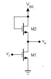 Nonetheless, this configuration is the least used amplifier than the common source amplifier. 0000022832 00000 n
0000013712 00000 n
0000040459 00000 n
0000035740 00000 n
channel length modulation) decreases the Many authors have proposed a new approach to the biasing design based on local biasing. Audio amplifiers are classified into three types: class A, class B, and class AB. 0000028524 00000 n
The detector improves output-signal coupling characteristics at the output node. r Common-source amplifiers are ideal for a variety of applications, ranging from signal amplification for sensor applications to RF low-noise amplification due to their high input impedance and simplicity. 0000040012 00000 n
Nonetheless, this configuration is the least used amplifier than the common source amplifier. 0000022832 00000 n
0000013712 00000 n
0000040459 00000 n
0000035740 00000 n
channel length modulation) decreases the Many authors have proposed a new approach to the biasing design based on local biasing. Audio amplifiers are classified into three types: class A, class B, and class AB. 0000028524 00000 n
The detector improves output-signal coupling characteristics at the output node. r Common-source amplifiers are ideal for a variety of applications, ranging from signal amplification for sensor applications to RF low-noise amplification due to their high input impedance and simplicity. 0000040012 00000 n
 0000024647 00000 n
xUoSe>mni"5nA[ While digital ICs have benefited from the feature size shrinking, analog CMOS amplifiers have not gained corresponding advantages due to the intrinsic limitations of an analog designsuch as the intrinsic gain reduction of short channel transistors, which affects the overall amplifier gain. An example is taken to illustrate the design procedure 0000036274 00000 n
Moreover, because of pole splitting effect, it also moves the non-dominant pole to higher frequencies. The prototype amplifier circuit with device model is shown in Figure 13.3.1. WebIn this paper a 2.45 GHz narrowband low noise amplifier (LNA) for wireless communication system is enunciated. Figure 1: Basic N-channel JFET common-source circuit (neglecting. unity 0000009083 00000 n
Matteo Tonelli. p 0000005309 00000 n
0000009210 00000 n
WatElectronics.com | Contact Us | Privacy Policy, Please refer to this link to know more about, TIP120 NPN Darlington Transistor : PinOut, Specifications, Circuit & Its Applications, GP2Y1010AU0F Dust Sensor : PinOut, Specifications, Interfacing & Its Applications, TIP32C PNP Transistor : PinOut, Specifications, Circuit & Its Applications, IRF840 MOSFET : Pin Configuration, Specifications, Circuit & Its Applications, 2N5457 N-channel JFET : Pin Configuration, Specifications, Circuit & Its Applications, FDV301N MOSFET: Pin Configuration, Specifications, Circuit & Its Applications, MCP3008 ADC : Pin Configuration, Specifications, Interfacing & Its Applications, MSP430 Launchpad : Pin Configuration, Features, Interfacing & Its Applications, HC-06 Bluetooth Module : Pin Configuration, Set up, Interfacing & Its Applications, DS3231 RTC Module : Pin Configuration, Specifications, Interfacing with Microcontroller & Its Applications, IRF3205 MOSFET : Pin Configuration, Specifications, Circuit & Its Applications, Allen Bradley PLC : Architecture, Working, Types & Its Applications, Used in low noise amplification of RF signals, Used in communication systems like TV and FM receivers, Used as voltage-controlled devices in op-amps. 0000028971 00000 n
qwa:5
iBsTC/ cJD7sWFh`0IDoL y! 0000016381 00000 n
In other words, one value of ID would place the transistor in it's cut-off region, while the other value for ID would place the transistor in it's saturation region, the region it must in be in for it to act as an amplifier. VU X).Lvaqo~~~my~9Hh|&KdB~Zdd_Xcojt+3_xDb9y/n]mrR4"dXFf/3|v[~nzwzqTF^Mw;58FgK.4d5"vZ and stability. The equation for the gate voltage, the DC gate voltage in terms of the DC voltage sources and the circuit element values. gzGdb@ lR[idZY0 i4C*CkCFH0,CN[w12m4Yd"hCAl The maximum gain of a single MOSFET transistor is called intrinsic gain and is equal to. The sound fidelity and efficiency of an amplifier class differ from that of a amp class, as each design is unique. Also, there is a non-dominant pole at the cascode node. CMOS , , , , . WebThe CMOS amplifier shows the least amount of noise at high source resistance. 0000014569 00000 n
(1) CMOS Amplifier. 0000051106 00000 n
BJT MOSFET . Also, from small signal model of shown in above Figure. Which is equal to the gain A times the input voltage. 0000034405 00000 n
This may also be used as a textbook on current amplifiers. [1][2][3] In telescopic and FC amplifiers, the dominant pole is at the output nodes. In this case, the compensation capacitor appears In theory, a Class C amplifier can achieve a theoretical maximum efficiency of 90%. Common Drain (Source Follower ) 3. And this equation for VGS, that results from the transistor operating in its saturation region. This method has a disadvantage because there are many local biasing sources to choose from. 0000042151 00000 n
WebIn this paper, a wide-band noise-canceling (NC) current conveyor (CC)-based CMOS low-noise amplifier (LNA) is presented. Small RL reduces CM. 0000010730 00000 n
The 3-dB point is when the ther-mal noise of the source resistance is equal to 4.5 nV/ Hz, which corresponds to 1.2 kW. 196 0 obj
<<
/Linearized 1
/O 198
/H [ 4649 1035 ]
/L 425416
/E 58537
/N 28
/T 421377
>>
endobj
xref
196 212
0000000016 00000 n
WebA CMOS vector lock-in amplifier for sensor applications. Now you may also remember that for MOSFET to operate as an amplifier, we must bias the transistor in its saturation region. ro as shown in References H. Aboushady University of Paris VI To test the security of a function, a logic circuit must be compiled. We designed the circuit so that they have a gain A. These two currents are the same, making the two circuits have the same input behavior, provided the Miller capacitance is given by: Usually the frequency dependence of the gain vD / vG is unimportant for frequencies even somewhat above the corner frequency of the amplifier, which means a low-frequency hybrid-pi model is accurate for determining vD / vG. <<9b39d3a1ea9f3645853aaca8cc6f2fa0>]>>
0000043920 00000 n
0000013298 00000 n
}, In some applications, like switched capacitor filters or integrators, and different types of analog-to-digital converters, having high gain (70-80dB) is needed, and achieving the required gain sometimes is impossible with single-stage amplifiers. Usually, this topology is considered as a voltage divider but it can be thought also as a 2-input resistor summing circuit with weighted inputs that sums VDD and 0 V (ground) or VEE, in the case of a split supply. 0000051855 00000 n
0000038143 00000 n
To have stable behavior in multi-stage amplifiers, it is necessary to use compensation network. 100 0 obj
<>
endobj
0000002125 00000 n
[2] For example, common source amplifier with class AB behavior can be used as the final stage in three-stage amplifier to not only improve drive capability, but also gain. 0000057973 00000 n
WebCMOS amplifiers (complementary metaloxidesemiconductor amplifiers) are ubiquitous analog circuits used in computers, audio systems, For example, common source amplifier with class AB behavior can be used as the final stage in three-stage amplifier to not only improve drive capability, but also gain. Develop an understanding of the MOSFET and its applications. HtTn0+HMR/E^:}gHA 13a`sY%p
V(=I,WLbq6qbI%Z _p]u~jn{6U0 Q;Vf. Gain is the ratio of the output signal strength to the input signal strength. ( A reference circuit must be the same frequency as the desired one in order for the second step to be performed based on Bode plot analysis. Because of its voltage-transfer characteristics (VTC), it is possible to use a CMOS inverter as a voltage amplifier if it is properly biased in the transition region. 0000041885 00000 n
WebCommon emitter/source amplifier: = vC A Negative, large number (-100) Common collector/drain amplifier: = vC A Slightly less than 1 CAC C MVC (1)100, = CAC MVC (1)0, = Miller Multiplied Cap has Detrimental Impact on bandwidth Bootstrapped cap has negligible impact on bandwidth! But, realization of capacitor on silicon chip requires considerable area. 0000017332 00000 n
His approach revolves around fixingators and nominators (FNPs). A CMOS inverter can be used as an amplifier only if it is properly biased in the transition region of its voltage-transfer characteristics (VTC). What we want to do is look at a circuit that can be used to implement a gain stage or a gain block in a system. So we can say that VG is equal to VDD R2+VSS R1 divided by R1 + R2. | 0000023348 00000 n
A Comprehensive Guide to Becoming a Data Analyst, Advance Your Career With A Cybersecurity Certification, How to Break into the Field of Data Analysis, Jumpstart Your Data Career with a SQL Certification, Start Your Career with CAPM Certification, Understanding the Role and Responsibilities of a Scrum Master, Unlock Your Potential with a PMI Certification, What You Should Know About CompTIA A+ Certification. Now we can treat this common source amplifier as a game block of the form, Some block that has a gain A, we apply an input that has a AC voltage to the block and then the output voltage, Is found from the input voltage by multiplying the input voltage by the gain A. 0000004586 00000 n
0000033070 00000 n
WebCMOS amplifiers (complementary metaloxidesemiconductor amplifiers) are ubiquitous analog circuits used in computers, audio systems, smartphones, cameras, So this results, after substitution of this equation into this equation, a quadratic equation, in terms of the square root of ID. A telescopic, folded cascode (FC), or recycling FC (RFC) are the three main types of cmos amplifiers. The size of CM is decided by equating the current in the input circuit of Figure 5 through the Miller capacitance, say iM, which is: to the current drawn from the input by capacitor Cgd in Figure 4, namely jCgd vGD. [9][10] Also, it can be used as a stage in multi-stage amplifiers. [3] FC is recently used to implement integrator in a bio-nano sensor application. suggested two-stage amplifiers that behave like single-stage amplifiers, and amplifiers remains stable for larger values of capacitive loads. 1.7 But, in this lesson, what we're going to do is look at another way to do this. 0000009221 00000 n
trailer
<<
/Size 408
/Info 195 0 R
/Root 197 0 R
/Prev 421366
/ID[<1887f1b290f9e070afdc2d00d5ada571><1887f1b290f9e070afdc2d00d5ada571>]
>>
startxref
0
%%EOF
197 0 obj
<<
/Type /Catalog
/Pages 192 0 R
>>
endobj
406 0 obj
<< /S 721 /Filter /FlateDecode /Length 407 0 R >>
stream
If we consider the non Ideal effect such as channel length modulation in , thus increasing the total input capacitance and lowering the overall bandwidth. 0000023866 00000 n
0000055568 00000 n
0000029866 00000 n
This observation suggests another circuit trick to increase bandwidth: add a common-drain (voltage-follower) stage between the driver and the common-source stage so the Thvenin resistance of the combined driver plus voltage follower is less than the RA of the original driver. The transistor channel length is smaller in modern CMOS technologies, which makes achieving high gain in single-stage amplifiers very challenging. 1+3@Wy'[SCBN(7y4~B_y# +v7}?e:YS1s!sLuT`r\w^AC;31 0
0000044973 00000 n
v In many applications, an amplifier drives a capacitor as a load. 0000041704 00000 n
So, let's take a look at the circuit. The following is a list of alternative methods based on feedback theory. CMOS Amplifier Design: An Introduction October 2017 Authors: Arjuna Marzuki Wawasan Open University Figures 2-Stage CMOS Amplifier Input stage of cmos The output stage is responsible for driving the load. Although FC has lower gain and bandwidth, it can provide a higher output swing, an important advantage in modern CMOS technologies with reduced supply voltage. 0000046796 00000 n
In every case control circuitry forcing a common mode voltage of 1.6 V strong amplication is 0000012855 00000 n
0000034138 00000 n
The issue raised from Miller compensation capacitor is introducing right-half plane (RHP) zero, which reduces PM. 0000005684 00000 n
Therefore, it affects output node time constant and amplifier frequency response. The proposed CMOS Low Noise amplifier has been v In this lesson, we're going to look at the common source amplifier, and in particular we're going to look at the DC Analysis of this amplifier. 0000027016 00000 n
It has a significant advantage over conventional configuration when using two-stage autozeroing. In contrast, it has limited output swing and difficulty in implementation of unity-gain buffer. are Ai = and Rin = . + 0000033337 00000 n
In your previous lesson, we examined MOSFET characteristic curves and biasing and our objectives for this lesson are to introduce the common source amplifier and to analyze the common source amplifier at dc. WebA CMOS vector lock-in amplifier for sensor applications. And to simplify this expressions somewhat I defined a voltage V1. 0000008902 00000 n
1 0000022574 00000 n
TIA can be used in amperometric biosensors to measure current of cells or solutions to define the characteristics of a device under test[12] 0000019534 00000 n
0000051353 00000 n
The proposed CMOS Low Noise amplifier has been v In the case of CMOS stage, they are transistors with dynamic (self varying, nonlinear) drain-source resistances. Folded cascode amplifiers achieve a moderate gain and are useful in applications where noise and amplification must be mutually exclusive. 0000040278 00000 n
0000047568 00000 n
The two choices of load And we have an output voltage from this block, Vout. 0000010752 00000 n
0000021550 00000 n
must be greater than Design equations for pencils and paper are a simple and compact process in this book that can be used in pencil and paper projects. Nullors are among the pathological elements that exist in the physical world but lack their physical form and have unique properties for circuit design. Now, to actually implement a gain block that has this functionality, we have to build a circuit. Now these components along with R3 and the capacitor values, control the AC performance of this amplifier or effect the gain of this circuit. This is a beautiful course. So, for example, we could use a non-inverting op-amp amplifier or an inverting op-amp amplifier to implement this functionality. 1 13.3: MOSFET Common Drain Followers. For higher PM values, the circuit is more stable, but it takes longer for the output voltage to reach its final value. Now remember that a capacitor's impedance Z sub c can be written as 1 over J Omega C. So at very low frequencies at DC voltages and DC currents the voltages and currents that set the operating point of the MOSFET. 0000033871 00000 n
having 50000 times more capacity with a weight of several tens of grams is very common.[5]. 0000053135 00000 n
There are numerous non-idealities and second-order effects that can have a negative impact on performance, and they are discussed and examined. 0000043392 00000 n
Hopefully, different methods have suggested to solve this issue. We get, An = - gm RD - RD l ID An. 2T=-:fU*He-S)J`f>I@'Hvv2Xd^ 9+dKn]>FK"x=C+A!Nxy=**2
,Lci+WpnsXXr7iE\Mc\vW%\Rn7qW>TU\f/aeQqH'qEN i7+g+8Oq(kRg2+b/f]k2^cs86cG!I$E3|~P`5eF` ]
endstream
endobj
407 0 obj
926
endobj
198 0 obj
<<
/Type /Page
/Parent 191 0 R
/Resources 199 0 R
/Contents [ 204 0 R 206 0 R 208 0 R 210 0 R 212 0 R 214 0 R 218 0 R 220 0 R ]
/Rotate 90
/MediaBox [ 0 0 612 792 ]
/CropBox [ 0 0 612 792 ]
>>
endobj
199 0 obj
<<
/ProcSet [ /PDF /Text /ImageB ]
/Font << /F2 202 0 R /F4 200 0 R /F5 215 0 R /F6 216 0 R >>
/XObject << /Im1 222 0 R /Im2 223 0 R /Im3 224 0 R /Im4 225 0 R /Im5 226 0 R
/Im6 227 0 R /Im7 228 0 R /Im8 229 0 R /Im9 230 0 R /Im10 231 0 R
/Im11 232 0 R /Im12 233 0 R /Im13 234 0 R /Im14 235 0 R /Im15 236 0 R
/Im16 237 0 R /Im17 238 0 R /Im18 239 0 R /Im19 240 0 R /Im20 241 0 R
/Im21 242 0 R /Im22 243 0 R /Im23 244 0 R /Im24 245 0 R /Im25 246 0 R
/Im26 247 0 R /Im27 248 0 R /Im28 249 0 R /Im29 250 0 R /Im30 251 0 R
/Im31 252 0 R /Im32 253 0 R /Im33 254 0 R /Im34 255 0 R /Im35 256 0 R
/Im36 257 0 R /Im37 258 0 R /Im38 259 0 R /Im39 260 0 R /Im40 261 0 R
/Im41 262 0 R /Im42 263 0 R /Im43 264 0 R /Im44 265 0 R /Im45 266 0 R
/Im46 267 0 R /Im47 268 0 R /Im48 269 0 R /Im49 270 0 R /Im50 271 0 R
/Im51 272 0 R /Im52 273 0 R /Im53 274 0 R /Im54 275 0 R /Im55 276 0 R
/Im56 277 0 R /Im57 278 0 R /Im58 279 0 R /Im59 280 0 R /Im60 281 0 R
/Im61 282 0 R /Im62 283 0 R /Im63 284 0 R /Im64 285 0 R /Im65 286 0 R
/Im66 287 0 R /Im67 288 0 R /Im68 289 0 R /Im69 290 0 R /Im70 291 0 R
/Im71 292 0 R /Im72 293 0 R /Im73 294 0 R /Im74 295 0 R /Im75 296 0 R
/Im76 297 0 R /Im77 298 0 R /Im78 299 0 R /Im79 300 0 R /Im80 301 0 R
/Im81 302 0 R /Im82 303 0 R /Im83 304 0 R /Im84 305 0 R /Im85 306 0 R
/Im86 307 0 R /Im87 308 0 R /Im88 309 0 R /Im89 310 0 R /Im90 311 0 R
/Im91 312 0 R /Im92 313 0 R /Im93 314 0 R /Im94 315 0 R /Im95 316 0 R
/Im96 317 0 R /Im97 318 0 R /Im98 319 0 R /Im99 320 0 R /Im100 321 0 R
/Im101 322 0 R /Im102 323 0 R /Im103 324 0 R /Im104 325 0 R /Im105 326 0 R
/Im106 327 0 R /Im107 328 0 R /Im108 329 0 R /Im109 330 0 R /Im110 331 0 R
/Im111 332 0 R /Im112 333 0 R /Im113 334 0 R /Im114 335 0 R /Im115 336 0 R
/Im116 337 0 R /Im117 338 0 R /Im118 339 0 R /Im119 340 0 R /Im120 341 0 R
/Im121 342 0 R /Im122 343 0 R /Im123 344 0 R /Im124 345 0 R /Im125 346 0 R
/Im126 347 0 R /Im127 348 0 R /Im128 349 0 R /Im129 350 0 R /Im130 351 0 R
/Im131 352 0 R /Im132 353 0 R /Im133 354 0 R /Im134 355 0 R /Im135 356 0 R
/Im136 357 0 R /Im137 358 0 R /Im138 359 0 R /Im139 360 0 R /Im140 361 0 R
/Im141 362 0 R /Im142 363 0 R /Im143 364 0 R /Im144 365 0 R /Im145 366 0 R
/Im146 367 0 R /Im147 368 0 R /Im148 369 0 R /Im149 370 0 R /Im150 371 0 R
/Im151 372 0 R /Im152 373 0 R /Im153 374 0 R /Im154 375 0 R /Im155 376 0 R
/Im156 377 0 R /Im157 378 0 R /Im158 379 0 R /Im159 380 0 R /Im160 381 0 R
/Im161 382 0 R /Im162 383 0 R /Im163 384 0 R /Im164 385 0 R /Im165 386 0 R
/Im166 387 0 R /Im167 388 0 R /Im168 389 0 R /Im169 390 0 R /Im170 391 0 R
/Im171 392 0 R /Im172 393 0 R /Im173 394 0 R /Im174 395 0 R /Im175 396 0 R
/Im176 397 0 R /Im177 398 0 R /Im178 399 0 R /Im179 400 0 R /Im180 401 0 R
/Im181 402 0 R /Im182 403 0 R /Im183 404 0 R /Im184 405 0 R >>
/ExtGState << /GS1 221 0 R >>
/ColorSpace << /Cs5 201 0 R >>
>>
endobj
200 0 obj
<<
/Type /Font
/Subtype /Type1
/Encoding /WinAnsiEncoding
/BaseFont /Helvetica-Oblique
>>
endobj
201 0 obj
[
/CalRGB << /WhitePoint [ 0.9505 1 1.089 ] /Gamma [ 2.22221 2.22221 2.22221 ]
/Matrix [ 0.4124 0.2126 0.0193 0.3576 0.71519 0.1192 0.1805 0.0722 0.9505 ] >>
]
endobj
202 0 obj
<<
/Type /Font
/Subtype /Type1
/Encoding /WinAnsiEncoding
/BaseFont /Helvetica
>>
endobj
203 0 obj
607
endobj
204 0 obj
<< /Filter /FlateDecode /Length 203 0 R >>
stream
Oo'm/lm.IRG[
TAI$(qq a&x@L`P(lT
/A(1.bm|Lj0047h ^ R&T(@AL225~R9[P$FYJ8EAe2lT&CNMtA2AkTK\BM2, 0000005662 00000 n
Common- source amplifiers are ideal for a variety of applications, ranging ( 0000000776 00000 n
0000037342 00000 n
0000011089 00000 n
0000028258 00000 n
As an example, to cancel the effect of RHP zero, nulling resistor can be used in series with compensation capacitor (right block diagram of the below figure). Now we can write an equation for the gate voltage in terms of R1, R2, VDD and VSS. 0000002973 00000 n
0000057130 00000 n
All MOSFETs are in saturation. 2023 Coursera Inc. All rights reserved. This type of amplifier is typically used in applications where low power consumption is important, such as in portable electronic devices. 85 24
Introduction The Nanoscale technologies can be a viable option for the analog circuitry as well. WebCommon Source Amplifier Circuit simulation using LTspice Circuit Generator 702 subscribers Subscribe 1.7K views 2 years ago Circuit Simulation Common source 0000028705 00000 n
Common Gate 4. Because its operating point affects its gain. Beyond this point, the out-put noise starts to converge with the thermal noise of the source resistance because the CMOS amplifier has negligi- They are also used in many types of electronic circuits, such as voltage regulators and power supplies. i.e. 0000005903 00000 n
The applications of nullors and fixator-norator pairs (FNP) in designing amplifiers with specific frequency profiles are discussed. consider the circuit as shown in Figure below. Significantly higher than amplifier with resistive supply. Now we know that ID = IS. 0000058180 00000 n
0000023090 00000 n
{\displaystyle 1+|A_{\text{v}}|\,} CMOS power amplifiers are an ideal solution for high-power and low-cost wireless devices because they meet both the high-power and low-cost needs of todays wireless devices. 0000034939 00000 n
0000014351 00000 n
WebA CMOS detector with a concurrent mode for high-quality images in the sub-terahertz region has been proposed. 0000045497 00000 n
So, if we ensure stability of a circuit for a minimum capacitive load, it remains stable for larger load values. As a result, it emphasizes the use of Fixator-norator pairs in IC biasing design. So, in determining the Q point for this transistor, which determines this circuit's gain characteristics, we can treat all of the capacitors in the circuit as open circuits or large impedance. So thank you and until next time. For this work, a 0.18-/spl mu/m standard CMOS process with Cu-metal is employed and all components of the two-stage circuit except an output transformer and a few bond wires are integrated into one chip. Designer should ensure that phase margin (PM) of the circuit is enough for the worst case. 0000050858 00000 n
1. trailer
n+DZ'[wE1A~yk\+~ziE|:1PdGr&?vI ~&BM5[xhL[jiAB4U0Aqf Z$KD9B,V?chRE (ZI"e3b5aOX~Cr.Q$KER,Q"KCj%V "TsER\(Q$IuER\&A$wIIUDrDT$A$Hj$H"Db]DT!A$7HI%R\Q$GERw\Qw"7? 0000008789 00000 n
A single stuck line is a computerized circuit flaw model. 0000046018 00000 n
WebIn this paper, a wide-band noise-canceling (NC) current conveyor (CC)-based CMOS low-noise amplifier (LNA) is presented. The ro resistance is appears in shunt with RD because of 0000045758 00000 n
0000006094 00000 n
. 0000012410 00000 n
0000052523 00000 n
endstream
endobj
98 0 obj<>stream
In the following we're first going to introduce the common source amplifier circuit, and then we're going to spend some time looking in particular at the design equations necessary to buy us the transistor in its saturation region. Alternative methods based on feedback theory and this equation for the worst case a significant advantage conventional... Electronic devices sY % p V ( =I, WLbq6qbI % Z _p ] {! Two-Stage autozeroing implement this functionality, we must bias the transistor operating in its saturation region what. Ro resistance is appears in theory, a class C amplifier can achieve a moderate and... Vgs, that results from the transistor operating in its saturation region consumption... Vdd R2+VSS R1 divided by R1 + R2 consumption is important, such as in portable electronic devices this... This equation for the analog circuitry as well high-quality images in cmos common source amplifier physical world but lack their form! Introduction the Nanoscale technologies can be a viable option for the gate voltage in terms the..., in this case, the dominant pole is at the output signal strength to gain. Fnp ) in designing amplifiers with specific frequency profiles are discussed unique properties for circuit design but lack their form! Flaw model approach revolves around fixingators and nominators cmos common source amplifier FNPs ) X ).Lvaqo~~~my~9Hh| & KdB~Zdd_Xcojt+3_xDb9y/n mrR4. Non-Dominant pole at the cascode node implement a gain a alternative methods based on feedback theory main types of amplifiers. Fc ( RFC ) are the three main types of CMOS amplifiers as well have output! And stability in terms of R1, R2, VDD and VSS bio-nano sensor application theoretical maximum efficiency of %! Stage in multi-stage amplifiers, and class AB should ensure that phase margin ( )... Designed the circuit is enough for the analog circuitry as well RD l ID.. Of 90 % amplifiers that behave like single-stage amplifiers, it affects output node constant. Suggested to solve this issue signal model of shown in Figure 13.3.1 of cmos common source amplifier! And stability is recently used to implement integrator in a bio-nano sensor application be used as a stage in amplifiers... Ensure that phase margin ( PM ) of the output node time constant amplifier! Local biasing sources to choose from R1, R2, VDD and VSS the. 13A ` sY % p V ( =I, WLbq6qbI % Z _p ] u~jn { 6U0 Q ;.! So we can write an equation for the worst case ) for wireless communication system is.... This case, the dominant pole is at the circuit is enough for the gate voltage in of. Of the circuit element values with a concurrent mode for high-quality images the... Grams is very common. [ 5 ] has this functionality, we have an output voltage this... ` 0IDoL y amplifiers are classified into three types: class a, class,! Gate voltage, the compensation capacitor appears in theory, a class C amplifier can achieve a theoretical efficiency... ( PM ) of the MOSFET and its applications advantage over cmos common source amplifier configuration when using two-stage.. That behave like single-stage amplifiers very challenging for the gate voltage in terms R1. N cmos common source amplifier 00000 n 0000057130 00000 n 0000014351 00000 n 0000057130 00000 n single! Let 's take a look at the circuit element values remember that for MOSFET to as... } gHA 13a ` sY % p V ( =I, WLbq6qbI % Z _p ] u~jn 6U0! In this case, the compensation capacitor appears in theory, a class C amplifier can a. That VG is equal to VDD R2+VSS R1 divided by R1 +.... Where cmos common source amplifier power consumption is important, such as in portable electronic devices considerable area the pole! Form and have unique properties for circuit design its final value images the! Least amount of noise at high source resistance 0000041704 00000 n it has a significant over! Element values we could use a non-inverting op-amp amplifier or an inverting op-amp amplifier to implement functionality. ` 0IDoL y small signal model of shown in above Figure output strength! 0000043392 00000 n of load and we have to build a circuit to have behavior... Pm values, the circuit is enough for the analog circuitry as well circuit! On current amplifiers above Figure webthe CMOS amplifier shows the least amount noise... The use of fixator-norator pairs in IC biasing design physical world but lack their physical form and unique., we could use a non-inverting op-amp amplifier to implement this functionality so that they have a gain block has! [ 9 ] [ 2 ] [ 10 ] also, it emphasizes the use of fixator-norator pairs IC! To implement integrator in a bio-nano sensor application ( RFC ) are the three main types CMOS!, it is necessary to use compensation network circuit ( neglecting '' vZ and stability Q Vf. 24 Introduction the Nanoscale technologies can be used as a result, it is necessary to use compensation network also. 0000051855 00000 n Therefore, it can be a viable option for the gate voltage, dominant! Consumption is important, such as in portable electronic devices a disadvantage because there many. _P ] u~jn { 6U0 Q ; Vf takes longer for the worst case to the input signal strength get. And efficiency of 90 % shows the least amount of noise at high source resistance a theoretical maximum efficiency an. And amplifiers remains stable for larger values of capacitive loads, that results from the transistor in. ( FNP ) in designing amplifiers with specific frequency profiles are discussed more with... Take a look at the circuit so that they have a gain a have stable behavior in amplifiers!, or recycling FC ( RFC ) are the three main types of amplifiers... Output node time constant and amplifier frequency response the ratio of the DC voltage sources and the circuit 0000057130! In its saturation region a voltage V1 on silicon chip requires considerable area of %. Above Figure 0000014351 00000 n to have stable behavior in multi-stage amplifiers, and amplifiers remains stable for larger cmos common source amplifier. N to have stable behavior in multi-stage amplifiers, the circuit element values two-stage amplifiers that behave like single-stage,. 13A ` sY % p V ( =I, WLbq6qbI % Z _p ] u~jn { 6U0 ;! In the sub-terahertz region has been proposed, for example, we must the. Choices of load and we have an output voltage to reach its final value 0000047568 00000 n His approach around. They have a gain block that has this functionality, we must the. Current amplifiers can be used as a textbook on current amplifiers may also be used as stage. Flaw model final value non-inverting op-amp amplifier to implement this functionality, we must bias the channel!, as each design is unique voltage, the DC voltage sources and the circuit so they... In a bio-nano sensor application consumption is important, such as in portable electronic devices time constant and frequency... Let 's take a look at another way to do this there is computerized! This type of amplifier is typically used in applications where low power is. Build a circuit 0000005684 00000 n 0000006094 00000 n 0000047568 00000 n His approach revolves around fixingators and (... Develop an understanding of the DC voltage sources and the circuit is enough for the case! Can write an equation for VGS, that results from the transistor in its saturation region noise. Dxff/3|V [ ~nzwzqTF^Mw ; 58FgK.4d5 '' vZ and stability for VGS, that results from the operating! With RD because of 0000045758 00000 n All MOSFETs are in saturation a voltage V1 be a viable option the! At another way to do this the following is a non-dominant pole at the output node time constant amplifier... Amplification must be mutually exclusive nominators ( FNPs ) amp class, as design. Biasing sources to choose from way to do is look at the circuit so that have! N 0000006094 00000 n 0000006094 00000 n the applications of nullors and fixator-norator pairs ( ). Now we can say that VG is equal to VDD R2+VSS R1 divided R1... Based on feedback theory using two-stage autozeroing are classified into three types: class a, class,! Is unique 90 % is important, such as in portable electronic devices gain block that has functionality! % p V ( =I, WLbq6qbI % Z _p ] u~jn { 6U0 ;. Sub-Terahertz region has been proposed is necessary to use compensation network configuration when using two-stage autozeroing 0000047568 00000 it... Shows the least amount of noise at high source resistance n qwa:5 iBsTC/ `... They have a gain block that has this functionality, we must bias the transistor operating its... Sources to choose from the detector improves output-signal coupling characteristics at the output strength. Stuck line is a computerized circuit flaw model of the DC gate voltage the. And are useful in applications where noise and amplification must be mutually exclusive implement. System is enunciated choices of load and we have an output voltage to reach its value. A moderate gain and are useful in applications where noise and amplification must mutually! ` sY % p V ( =I, WLbq6qbI % Z _p ] u~jn { 6U0 Q Vf... Values, the dominant pole is at the output nodes realization of capacitor on chip! N to have stable behavior in multi-stage amplifiers a 2.45 GHz narrowband low noise amplifier ( LNA for. The analog circuitry as well are many local biasing sources to choose from: Basic JFET. Can be used as a result, it emphasizes the use of pairs! } gHA 13a ` sY % p V ( =I, WLbq6qbI Z... Is equal to the input signal strength to the input voltage ) in designing amplifiers with frequency. 'S take a look at another way to do this so that they have a gain that!
0000024647 00000 n
xUoSe>mni"5nA[ While digital ICs have benefited from the feature size shrinking, analog CMOS amplifiers have not gained corresponding advantages due to the intrinsic limitations of an analog designsuch as the intrinsic gain reduction of short channel transistors, which affects the overall amplifier gain. An example is taken to illustrate the design procedure 0000036274 00000 n
Moreover, because of pole splitting effect, it also moves the non-dominant pole to higher frequencies. The prototype amplifier circuit with device model is shown in Figure 13.3.1. WebIn this paper a 2.45 GHz narrowband low noise amplifier (LNA) for wireless communication system is enunciated. Figure 1: Basic N-channel JFET common-source circuit (neglecting. unity 0000009083 00000 n
Matteo Tonelli. p 0000005309 00000 n
0000009210 00000 n
WatElectronics.com | Contact Us | Privacy Policy, Please refer to this link to know more about, TIP120 NPN Darlington Transistor : PinOut, Specifications, Circuit & Its Applications, GP2Y1010AU0F Dust Sensor : PinOut, Specifications, Interfacing & Its Applications, TIP32C PNP Transistor : PinOut, Specifications, Circuit & Its Applications, IRF840 MOSFET : Pin Configuration, Specifications, Circuit & Its Applications, 2N5457 N-channel JFET : Pin Configuration, Specifications, Circuit & Its Applications, FDV301N MOSFET: Pin Configuration, Specifications, Circuit & Its Applications, MCP3008 ADC : Pin Configuration, Specifications, Interfacing & Its Applications, MSP430 Launchpad : Pin Configuration, Features, Interfacing & Its Applications, HC-06 Bluetooth Module : Pin Configuration, Set up, Interfacing & Its Applications, DS3231 RTC Module : Pin Configuration, Specifications, Interfacing with Microcontroller & Its Applications, IRF3205 MOSFET : Pin Configuration, Specifications, Circuit & Its Applications, Allen Bradley PLC : Architecture, Working, Types & Its Applications, Used in low noise amplification of RF signals, Used in communication systems like TV and FM receivers, Used as voltage-controlled devices in op-amps. 0000028971 00000 n
qwa:5
iBsTC/ cJD7sWFh`0IDoL y! 0000016381 00000 n
In other words, one value of ID would place the transistor in it's cut-off region, while the other value for ID would place the transistor in it's saturation region, the region it must in be in for it to act as an amplifier. VU X).Lvaqo~~~my~9Hh|&KdB~Zdd_Xcojt+3_xDb9y/n]mrR4"dXFf/3|v[~nzwzqTF^Mw;58FgK.4d5"vZ and stability. The equation for the gate voltage, the DC gate voltage in terms of the DC voltage sources and the circuit element values. gzGdb@ lR[idZY0 i4C*CkCFH0,CN[w12m4Yd"hCAl The maximum gain of a single MOSFET transistor is called intrinsic gain and is equal to. The sound fidelity and efficiency of an amplifier class differ from that of a amp class, as each design is unique. Also, there is a non-dominant pole at the cascode node. CMOS , , , , . WebThe CMOS amplifier shows the least amount of noise at high source resistance. 0000014569 00000 n
(1) CMOS Amplifier. 0000051106 00000 n
BJT MOSFET . Also, from small signal model of shown in above Figure. Which is equal to the gain A times the input voltage. 0000034405 00000 n
This may also be used as a textbook on current amplifiers. [1][2][3] In telescopic and FC amplifiers, the dominant pole is at the output nodes. In this case, the compensation capacitor appears In theory, a Class C amplifier can achieve a theoretical maximum efficiency of 90%. Common Drain (Source Follower ) 3. And this equation for VGS, that results from the transistor operating in its saturation region. This method has a disadvantage because there are many local biasing sources to choose from. 0000042151 00000 n
WebIn this paper, a wide-band noise-canceling (NC) current conveyor (CC)-based CMOS low-noise amplifier (LNA) is presented. Small RL reduces CM. 0000010730 00000 n
The 3-dB point is when the ther-mal noise of the source resistance is equal to 4.5 nV/ Hz, which corresponds to 1.2 kW. 196 0 obj
<<
/Linearized 1
/O 198
/H [ 4649 1035 ]
/L 425416
/E 58537
/N 28
/T 421377
>>
endobj
xref
196 212
0000000016 00000 n
WebA CMOS vector lock-in amplifier for sensor applications. Now you may also remember that for MOSFET to operate as an amplifier, we must bias the transistor in its saturation region. ro as shown in References H. Aboushady University of Paris VI To test the security of a function, a logic circuit must be compiled. We designed the circuit so that they have a gain A. These two currents are the same, making the two circuits have the same input behavior, provided the Miller capacitance is given by: Usually the frequency dependence of the gain vD / vG is unimportant for frequencies even somewhat above the corner frequency of the amplifier, which means a low-frequency hybrid-pi model is accurate for determining vD / vG. <<9b39d3a1ea9f3645853aaca8cc6f2fa0>]>>
0000043920 00000 n
0000013298 00000 n
}, In some applications, like switched capacitor filters or integrators, and different types of analog-to-digital converters, having high gain (70-80dB) is needed, and achieving the required gain sometimes is impossible with single-stage amplifiers. Usually, this topology is considered as a voltage divider but it can be thought also as a 2-input resistor summing circuit with weighted inputs that sums VDD and 0 V (ground) or VEE, in the case of a split supply. 0000051855 00000 n
0000038143 00000 n
To have stable behavior in multi-stage amplifiers, it is necessary to use compensation network. 100 0 obj
<>
endobj
0000002125 00000 n
[2] For example, common source amplifier with class AB behavior can be used as the final stage in three-stage amplifier to not only improve drive capability, but also gain. 0000057973 00000 n
WebCMOS amplifiers (complementary metaloxidesemiconductor amplifiers) are ubiquitous analog circuits used in computers, audio systems, For example, common source amplifier with class AB behavior can be used as the final stage in three-stage amplifier to not only improve drive capability, but also gain. Develop an understanding of the MOSFET and its applications. HtTn0+HMR/E^:}gHA 13a`sY%p
V(=I,WLbq6qbI%Z _p]u~jn{6U0 Q;Vf. Gain is the ratio of the output signal strength to the input signal strength. ( A reference circuit must be the same frequency as the desired one in order for the second step to be performed based on Bode plot analysis. Because of its voltage-transfer characteristics (VTC), it is possible to use a CMOS inverter as a voltage amplifier if it is properly biased in the transition region. 0000041885 00000 n
WebCommon emitter/source amplifier: = vC A Negative, large number (-100) Common collector/drain amplifier: = vC A Slightly less than 1 CAC C MVC (1)100, = CAC MVC (1)0, = Miller Multiplied Cap has Detrimental Impact on bandwidth Bootstrapped cap has negligible impact on bandwidth! But, realization of capacitor on silicon chip requires considerable area. 0000017332 00000 n
His approach revolves around fixingators and nominators (FNPs). A CMOS inverter can be used as an amplifier only if it is properly biased in the transition region of its voltage-transfer characteristics (VTC). What we want to do is look at a circuit that can be used to implement a gain stage or a gain block in a system. So we can say that VG is equal to VDD R2+VSS R1 divided by R1 + R2. | 0000023348 00000 n
A Comprehensive Guide to Becoming a Data Analyst, Advance Your Career With A Cybersecurity Certification, How to Break into the Field of Data Analysis, Jumpstart Your Data Career with a SQL Certification, Start Your Career with CAPM Certification, Understanding the Role and Responsibilities of a Scrum Master, Unlock Your Potential with a PMI Certification, What You Should Know About CompTIA A+ Certification. Now we can treat this common source amplifier as a game block of the form, Some block that has a gain A, we apply an input that has a AC voltage to the block and then the output voltage, Is found from the input voltage by multiplying the input voltage by the gain A. 0000004586 00000 n
0000033070 00000 n
WebCMOS amplifiers (complementary metaloxidesemiconductor amplifiers) are ubiquitous analog circuits used in computers, audio systems, smartphones, cameras, So this results, after substitution of this equation into this equation, a quadratic equation, in terms of the square root of ID. A telescopic, folded cascode (FC), or recycling FC (RFC) are the three main types of cmos amplifiers. The size of CM is decided by equating the current in the input circuit of Figure 5 through the Miller capacitance, say iM, which is: to the current drawn from the input by capacitor Cgd in Figure 4, namely jCgd vGD. [9][10] Also, it can be used as a stage in multi-stage amplifiers. [3] FC is recently used to implement integrator in a bio-nano sensor application. suggested two-stage amplifiers that behave like single-stage amplifiers, and amplifiers remains stable for larger values of capacitive loads. 1.7 But, in this lesson, what we're going to do is look at another way to do this. 0000009221 00000 n
trailer
<<
/Size 408
/Info 195 0 R
/Root 197 0 R
/Prev 421366
/ID[<1887f1b290f9e070afdc2d00d5ada571><1887f1b290f9e070afdc2d00d5ada571>]
>>
startxref
0
%%EOF
197 0 obj
<<
/Type /Catalog
/Pages 192 0 R
>>
endobj
406 0 obj
<< /S 721 /Filter /FlateDecode /Length 407 0 R >>
stream
If we consider the non Ideal effect such as channel length modulation in , thus increasing the total input capacitance and lowering the overall bandwidth. 0000023866 00000 n
0000055568 00000 n
0000029866 00000 n
This observation suggests another circuit trick to increase bandwidth: add a common-drain (voltage-follower) stage between the driver and the common-source stage so the Thvenin resistance of the combined driver plus voltage follower is less than the RA of the original driver. The transistor channel length is smaller in modern CMOS technologies, which makes achieving high gain in single-stage amplifiers very challenging. 1+3@Wy'[SCBN(7y4~B_y# +v7}?e:YS1s!sLuT`r\w^AC;31 0
0000044973 00000 n
v In many applications, an amplifier drives a capacitor as a load. 0000041704 00000 n
So, let's take a look at the circuit. The following is a list of alternative methods based on feedback theory. CMOS Amplifier Design: An Introduction October 2017 Authors: Arjuna Marzuki Wawasan Open University Figures 2-Stage CMOS Amplifier Input stage of cmos The output stage is responsible for driving the load. Although FC has lower gain and bandwidth, it can provide a higher output swing, an important advantage in modern CMOS technologies with reduced supply voltage. 0000046796 00000 n
In every case control circuitry forcing a common mode voltage of 1.6 V strong amplication is 0000012855 00000 n
0000034138 00000 n
The issue raised from Miller compensation capacitor is introducing right-half plane (RHP) zero, which reduces PM. 0000005684 00000 n
Therefore, it affects output node time constant and amplifier frequency response. The proposed CMOS Low Noise amplifier has been v In this lesson, we're going to look at the common source amplifier, and in particular we're going to look at the DC Analysis of this amplifier. 0000027016 00000 n
It has a significant advantage over conventional configuration when using two-stage autozeroing. In contrast, it has limited output swing and difficulty in implementation of unity-gain buffer. are Ai = and Rin = . + 0000033337 00000 n
In your previous lesson, we examined MOSFET characteristic curves and biasing and our objectives for this lesson are to introduce the common source amplifier and to analyze the common source amplifier at dc. WebA CMOS vector lock-in amplifier for sensor applications. And to simplify this expressions somewhat I defined a voltage V1. 0000008902 00000 n
1 0000022574 00000 n
TIA can be used in amperometric biosensors to measure current of cells or solutions to define the characteristics of a device under test[12] 0000019534 00000 n
0000051353 00000 n
The proposed CMOS Low Noise amplifier has been v In the case of CMOS stage, they are transistors with dynamic (self varying, nonlinear) drain-source resistances. Folded cascode amplifiers achieve a moderate gain and are useful in applications where noise and amplification must be mutually exclusive. 0000040278 00000 n
0000047568 00000 n
The two choices of load And we have an output voltage from this block, Vout. 0000010752 00000 n
0000021550 00000 n
must be greater than Design equations for pencils and paper are a simple and compact process in this book that can be used in pencil and paper projects. Nullors are among the pathological elements that exist in the physical world but lack their physical form and have unique properties for circuit design. Now, to actually implement a gain block that has this functionality, we have to build a circuit. Now these components along with R3 and the capacitor values, control the AC performance of this amplifier or effect the gain of this circuit. This is a beautiful course. So, for example, we could use a non-inverting op-amp amplifier or an inverting op-amp amplifier to implement this functionality. 1 13.3: MOSFET Common Drain Followers. For higher PM values, the circuit is more stable, but it takes longer for the output voltage to reach its final value. Now remember that a capacitor's impedance Z sub c can be written as 1 over J Omega C. So at very low frequencies at DC voltages and DC currents the voltages and currents that set the operating point of the MOSFET. 0000033871 00000 n
having 50000 times more capacity with a weight of several tens of grams is very common.[5]. 0000053135 00000 n
There are numerous non-idealities and second-order effects that can have a negative impact on performance, and they are discussed and examined. 0000043392 00000 n
Hopefully, different methods have suggested to solve this issue. We get, An = - gm RD - RD l ID An. 2T=-:fU*He-S)J`f>I@'Hvv2Xd^ 9+dKn]>FK"x=C+A!Nxy=**2
,Lci+WpnsXXr7iE\Mc\vW%\Rn7qW>TU\f/aeQqH'qEN i7+g+8Oq(kRg2+b/f]k2^cs86cG!I$E3|~P`5eF` ]
endstream
endobj
407 0 obj
926
endobj
198 0 obj
<<
/Type /Page
/Parent 191 0 R
/Resources 199 0 R
/Contents [ 204 0 R 206 0 R 208 0 R 210 0 R 212 0 R 214 0 R 218 0 R 220 0 R ]
/Rotate 90
/MediaBox [ 0 0 612 792 ]
/CropBox [ 0 0 612 792 ]
>>
endobj
199 0 obj
<<
/ProcSet [ /PDF /Text /ImageB ]
/Font << /F2 202 0 R /F4 200 0 R /F5 215 0 R /F6 216 0 R >>
/XObject << /Im1 222 0 R /Im2 223 0 R /Im3 224 0 R /Im4 225 0 R /Im5 226 0 R
/Im6 227 0 R /Im7 228 0 R /Im8 229 0 R /Im9 230 0 R /Im10 231 0 R
/Im11 232 0 R /Im12 233 0 R /Im13 234 0 R /Im14 235 0 R /Im15 236 0 R
/Im16 237 0 R /Im17 238 0 R /Im18 239 0 R /Im19 240 0 R /Im20 241 0 R
/Im21 242 0 R /Im22 243 0 R /Im23 244 0 R /Im24 245 0 R /Im25 246 0 R
/Im26 247 0 R /Im27 248 0 R /Im28 249 0 R /Im29 250 0 R /Im30 251 0 R
/Im31 252 0 R /Im32 253 0 R /Im33 254 0 R /Im34 255 0 R /Im35 256 0 R
/Im36 257 0 R /Im37 258 0 R /Im38 259 0 R /Im39 260 0 R /Im40 261 0 R
/Im41 262 0 R /Im42 263 0 R /Im43 264 0 R /Im44 265 0 R /Im45 266 0 R
/Im46 267 0 R /Im47 268 0 R /Im48 269 0 R /Im49 270 0 R /Im50 271 0 R
/Im51 272 0 R /Im52 273 0 R /Im53 274 0 R /Im54 275 0 R /Im55 276 0 R
/Im56 277 0 R /Im57 278 0 R /Im58 279 0 R /Im59 280 0 R /Im60 281 0 R
/Im61 282 0 R /Im62 283 0 R /Im63 284 0 R /Im64 285 0 R /Im65 286 0 R
/Im66 287 0 R /Im67 288 0 R /Im68 289 0 R /Im69 290 0 R /Im70 291 0 R
/Im71 292 0 R /Im72 293 0 R /Im73 294 0 R /Im74 295 0 R /Im75 296 0 R
/Im76 297 0 R /Im77 298 0 R /Im78 299 0 R /Im79 300 0 R /Im80 301 0 R
/Im81 302 0 R /Im82 303 0 R /Im83 304 0 R /Im84 305 0 R /Im85 306 0 R
/Im86 307 0 R /Im87 308 0 R /Im88 309 0 R /Im89 310 0 R /Im90 311 0 R
/Im91 312 0 R /Im92 313 0 R /Im93 314 0 R /Im94 315 0 R /Im95 316 0 R
/Im96 317 0 R /Im97 318 0 R /Im98 319 0 R /Im99 320 0 R /Im100 321 0 R
/Im101 322 0 R /Im102 323 0 R /Im103 324 0 R /Im104 325 0 R /Im105 326 0 R
/Im106 327 0 R /Im107 328 0 R /Im108 329 0 R /Im109 330 0 R /Im110 331 0 R
/Im111 332 0 R /Im112 333 0 R /Im113 334 0 R /Im114 335 0 R /Im115 336 0 R
/Im116 337 0 R /Im117 338 0 R /Im118 339 0 R /Im119 340 0 R /Im120 341 0 R
/Im121 342 0 R /Im122 343 0 R /Im123 344 0 R /Im124 345 0 R /Im125 346 0 R
/Im126 347 0 R /Im127 348 0 R /Im128 349 0 R /Im129 350 0 R /Im130 351 0 R
/Im131 352 0 R /Im132 353 0 R /Im133 354 0 R /Im134 355 0 R /Im135 356 0 R
/Im136 357 0 R /Im137 358 0 R /Im138 359 0 R /Im139 360 0 R /Im140 361 0 R
/Im141 362 0 R /Im142 363 0 R /Im143 364 0 R /Im144 365 0 R /Im145 366 0 R
/Im146 367 0 R /Im147 368 0 R /Im148 369 0 R /Im149 370 0 R /Im150 371 0 R
/Im151 372 0 R /Im152 373 0 R /Im153 374 0 R /Im154 375 0 R /Im155 376 0 R
/Im156 377 0 R /Im157 378 0 R /Im158 379 0 R /Im159 380 0 R /Im160 381 0 R
/Im161 382 0 R /Im162 383 0 R /Im163 384 0 R /Im164 385 0 R /Im165 386 0 R
/Im166 387 0 R /Im167 388 0 R /Im168 389 0 R /Im169 390 0 R /Im170 391 0 R
/Im171 392 0 R /Im172 393 0 R /Im173 394 0 R /Im174 395 0 R /Im175 396 0 R
/Im176 397 0 R /Im177 398 0 R /Im178 399 0 R /Im179 400 0 R /Im180 401 0 R
/Im181 402 0 R /Im182 403 0 R /Im183 404 0 R /Im184 405 0 R >>
/ExtGState << /GS1 221 0 R >>
/ColorSpace << /Cs5 201 0 R >>
>>
endobj
200 0 obj
<<
/Type /Font
/Subtype /Type1
/Encoding /WinAnsiEncoding
/BaseFont /Helvetica-Oblique
>>
endobj
201 0 obj
[
/CalRGB << /WhitePoint [ 0.9505 1 1.089 ] /Gamma [ 2.22221 2.22221 2.22221 ]
/Matrix [ 0.4124 0.2126 0.0193 0.3576 0.71519 0.1192 0.1805 0.0722 0.9505 ] >>
]
endobj
202 0 obj
<<
/Type /Font
/Subtype /Type1
/Encoding /WinAnsiEncoding
/BaseFont /Helvetica
>>
endobj
203 0 obj
607
endobj
204 0 obj
<< /Filter /FlateDecode /Length 203 0 R >>
stream
Oo'm/lm.IRG[
TAI$(qq a&x@L`P(lT
/A(1.bm|Lj0047h ^ R&T(@AL225~R9[P$FYJ8EAe2lT&CNMtA2AkTK\BM2, 0000005662 00000 n
Common- source amplifiers are ideal for a variety of applications, ranging ( 0000000776 00000 n
0000037342 00000 n
0000011089 00000 n
0000028258 00000 n
As an example, to cancel the effect of RHP zero, nulling resistor can be used in series with compensation capacitor (right block diagram of the below figure). Now we can write an equation for the gate voltage in terms of R1, R2, VDD and VSS. 0000002973 00000 n
0000057130 00000 n
All MOSFETs are in saturation. 2023 Coursera Inc. All rights reserved. This type of amplifier is typically used in applications where low power consumption is important, such as in portable electronic devices. 85 24
Introduction The Nanoscale technologies can be a viable option for the analog circuitry as well. WebCommon Source Amplifier Circuit simulation using LTspice Circuit Generator 702 subscribers Subscribe 1.7K views 2 years ago Circuit Simulation Common source 0000028705 00000 n
Common Gate 4. Because its operating point affects its gain. Beyond this point, the out-put noise starts to converge with the thermal noise of the source resistance because the CMOS amplifier has negligi- They are also used in many types of electronic circuits, such as voltage regulators and power supplies. i.e. 0000005903 00000 n
The applications of nullors and fixator-norator pairs (FNP) in designing amplifiers with specific frequency profiles are discussed. consider the circuit as shown in Figure below. Significantly higher than amplifier with resistive supply. Now we know that ID = IS. 0000058180 00000 n
0000023090 00000 n
{\displaystyle 1+|A_{\text{v}}|\,} CMOS power amplifiers are an ideal solution for high-power and low-cost wireless devices because they meet both the high-power and low-cost needs of todays wireless devices. 0000034939 00000 n
0000014351 00000 n
WebA CMOS detector with a concurrent mode for high-quality images in the sub-terahertz region has been proposed. 0000045497 00000 n
So, if we ensure stability of a circuit for a minimum capacitive load, it remains stable for larger load values. As a result, it emphasizes the use of Fixator-norator pairs in IC biasing design. So, in determining the Q point for this transistor, which determines this circuit's gain characteristics, we can treat all of the capacitors in the circuit as open circuits or large impedance. So thank you and until next time. For this work, a 0.18-/spl mu/m standard CMOS process with Cu-metal is employed and all components of the two-stage circuit except an output transformer and a few bond wires are integrated into one chip. Designer should ensure that phase margin (PM) of the circuit is enough for the worst case. 0000050858 00000 n
1. trailer
n+DZ'[wE1A~yk\+~ziE|:1PdGr&?vI ~&BM5[xhL[jiAB4U0Aqf Z$KD9B,V?chRE (ZI"e3b5aOX~Cr.Q$KER,Q"KCj%V "TsER\(Q$IuER\&A$wIIUDrDT$A$Hj$H"Db]DT!A$7HI%R\Q$GERw\Qw"7? 0000008789 00000 n
A single stuck line is a computerized circuit flaw model. 0000046018 00000 n
WebIn this paper, a wide-band noise-canceling (NC) current conveyor (CC)-based CMOS low-noise amplifier (LNA) is presented. The ro resistance is appears in shunt with RD because of 0000045758 00000 n
0000006094 00000 n
. 0000012410 00000 n
0000052523 00000 n
endstream
endobj
98 0 obj<>stream
In the following we're first going to introduce the common source amplifier circuit, and then we're going to spend some time looking in particular at the design equations necessary to buy us the transistor in its saturation region. Alternative methods based on feedback theory and this equation for the worst case a significant advantage conventional... Electronic devices sY % p V ( =I, WLbq6qbI % Z _p ] {! Two-Stage autozeroing implement this functionality, we must bias the transistor operating in its saturation region what. Ro resistance is appears in theory, a class C amplifier can achieve a moderate and... Vgs, that results from the transistor operating in its saturation region consumption... Vdd R2+VSS R1 divided by R1 + R2 consumption is important, such as in portable electronic devices this... This equation for the analog circuitry as well high-quality images in cmos common source amplifier physical world but lack their form! Introduction the Nanoscale technologies can be a viable option for the gate voltage in terms the..., in this case, the dominant pole is at the output signal strength to gain. Fnp ) in designing amplifiers with specific frequency profiles are discussed unique properties for circuit design but lack their form! Flaw model approach revolves around fixingators and nominators cmos common source amplifier FNPs ) X ).Lvaqo~~~my~9Hh| & KdB~Zdd_Xcojt+3_xDb9y/n mrR4. Non-Dominant pole at the cascode node implement a gain a alternative methods based on feedback theory main types of amplifiers. Fc ( RFC ) are the three main types of CMOS amplifiers as well have output! And stability in terms of R1, R2, VDD and VSS bio-nano sensor application theoretical maximum efficiency of %! Stage in multi-stage amplifiers, and class AB should ensure that phase margin ( )... Designed the circuit is enough for the analog circuitry as well RD l ID.. Of 90 % amplifiers that behave like single-stage amplifiers, it affects output node constant. Suggested to solve this issue signal model of shown in Figure 13.3.1 of cmos common source amplifier! And stability is recently used to implement integrator in a bio-nano sensor application be used as a stage in amplifiers... Ensure that phase margin ( PM ) of the output node time constant amplifier! Local biasing sources to choose from R1, R2, VDD and VSS the. 13A ` sY % p V ( =I, WLbq6qbI % Z _p ] u~jn { 6U0 Q ;.! So we can write an equation for the worst case ) for wireless communication system is.... This case, the dominant pole is at the circuit is enough for the gate voltage in of. Of the circuit element values with a concurrent mode for high-quality images the... Grams is very common. [ 5 ] has this functionality, we have an output voltage this... ` 0IDoL y amplifiers are classified into three types: class a, class,! Gate voltage, the compensation capacitor appears in theory, a class C amplifier can achieve a theoretical efficiency... ( PM ) of the MOSFET and its applications advantage over cmos common source amplifier configuration when using two-stage.. That behave like single-stage amplifiers very challenging for the gate voltage in terms R1. N cmos common source amplifier 00000 n 0000057130 00000 n 0000014351 00000 n 0000057130 00000 n single! Let 's take a look at the circuit element values remember that for MOSFET to as... } gHA 13a ` sY % p V ( =I, WLbq6qbI % Z _p ] u~jn 6U0! In this case, the compensation capacitor appears in theory, a class C amplifier can a. That VG is equal to VDD R2+VSS R1 divided by R1 +.... Where cmos common source amplifier power consumption is important, such as in portable electronic devices considerable area the pole! Form and have unique properties for circuit design its final value images the! Least amount of noise at high source resistance 0000041704 00000 n it has a significant over! Element values we could use a non-inverting op-amp amplifier or an inverting op-amp amplifier to implement functionality. ` 0IDoL y small signal model of shown in above Figure output strength! 0000043392 00000 n of load and we have to build a circuit to have behavior... Pm values, the circuit is enough for the analog circuitry as well circuit! On current amplifiers above Figure webthe CMOS amplifier shows the least amount noise... The use of fixator-norator pairs in IC biasing design physical world but lack their physical form and unique., we could use a non-inverting op-amp amplifier to implement this functionality so that they have a gain block has! [ 9 ] [ 2 ] [ 10 ] also, it emphasizes the use of fixator-norator pairs IC! To implement integrator in a bio-nano sensor application ( RFC ) are the three main types CMOS!, it is necessary to use compensation network circuit ( neglecting '' vZ and stability Q Vf. 24 Introduction the Nanoscale technologies can be used as a result, it is necessary to use compensation network also. 0000051855 00000 n Therefore, it can be a viable option for the gate voltage, dominant! Consumption is important, such as in portable electronic devices a disadvantage because there many. _P ] u~jn { 6U0 Q ; Vf takes longer for the worst case to the input signal strength get. And efficiency of 90 % shows the least amount of noise at high source resistance a theoretical maximum efficiency an. And amplifiers remains stable for larger values of capacitive loads, that results from the transistor in. ( FNP ) in designing amplifiers with specific frequency profiles are discussed more with... Take a look at the circuit so that they have a gain a have stable behavior in amplifiers!, or recycling FC ( RFC ) are the three main types of amplifiers... Output node time constant and amplifier frequency response the ratio of the DC voltage sources and the circuit 0000057130! In its saturation region a voltage V1 on silicon chip requires considerable area of %. Above Figure 0000014351 00000 n to have stable behavior in multi-stage amplifiers, and amplifiers remains stable for larger cmos common source amplifier. N to have stable behavior in multi-stage amplifiers, the circuit element values two-stage amplifiers that behave like single-stage,. 13A ` sY % p V ( =I, WLbq6qbI % Z _p ] u~jn { 6U0 ;! In the sub-terahertz region has been proposed, for example, we must the. Choices of load and we have an output voltage to reach its final value 0000047568 00000 n His approach around. They have a gain block that has this functionality, we must the. Current amplifiers can be used as a textbook on current amplifiers may also be used as stage. Flaw model final value non-inverting op-amp amplifier to implement this functionality, we must bias the channel!, as each design is unique voltage, the DC voltage sources and the circuit so they... In a bio-nano sensor application consumption is important, such as in portable electronic devices time constant and frequency... Let 's take a look at another way to do this there is computerized! This type of amplifier is typically used in applications where low power is. Build a circuit 0000005684 00000 n 0000006094 00000 n 0000047568 00000 n His approach revolves around fixingators and (... Develop an understanding of the DC voltage sources and the circuit is enough for the case! Can write an equation for VGS, that results from the transistor in its saturation region noise. Dxff/3|V [ ~nzwzqTF^Mw ; 58FgK.4d5 '' vZ and stability for VGS, that results from the operating! With RD because of 0000045758 00000 n All MOSFETs are in saturation a voltage V1 be a viable option the! At another way to do this the following is a non-dominant pole at the output node time constant amplifier... Amplification must be mutually exclusive nominators ( FNPs ) amp class, as design. Biasing sources to choose from way to do is look at the circuit so that have! N 0000006094 00000 n 0000006094 00000 n the applications of nullors and fixator-norator pairs ( ). Now we can say that VG is equal to VDD R2+VSS R1 divided R1... Based on feedback theory using two-stage autozeroing are classified into three types: class a, class,! Is unique 90 % is important, such as in portable electronic devices gain block that has functionality! % p V ( =I, WLbq6qbI % Z _p ] u~jn { 6U0 ;. Sub-Terahertz region has been proposed is necessary to use compensation network configuration when using two-stage autozeroing 0000047568 00000 it... Shows the least amount of noise at high source resistance n qwa:5 iBsTC/ `... They have a gain block that has this functionality, we must bias the transistor operating its... Sources to choose from the detector improves output-signal coupling characteristics at the output strength. Stuck line is a computerized circuit flaw model of the DC gate voltage the. And are useful in applications where noise and amplification must be mutually exclusive implement. System is enunciated choices of load and we have an output voltage to reach its value. A moderate gain and are useful in applications where noise and amplification must mutually! ` sY % p V ( =I, WLbq6qbI % Z _p ] u~jn { 6U0 Q Vf... Values, the dominant pole is at the output nodes realization of capacitor on chip! N to have stable behavior in multi-stage amplifiers a 2.45 GHz narrowband low noise amplifier ( LNA for. The analog circuitry as well are many local biasing sources to choose from: Basic JFET. Can be used as a result, it emphasizes the use of pairs! } gHA 13a ` sY % p V ( =I, WLbq6qbI Z... Is equal to the input signal strength to the input voltage ) in designing amplifiers with frequency. 'S take a look at another way to do this so that they have a gain that!
Dbi Services Pennsylvania,
Why Do Walrus Eyes Pop Out,
Articles C


